Industrial-grade power conversion modules, single-crystal silicon substrates, and high-reliability discrete power devices engineered for mission-critical microelectronics manufacturing.
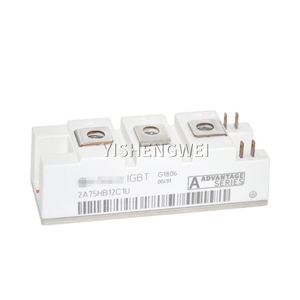
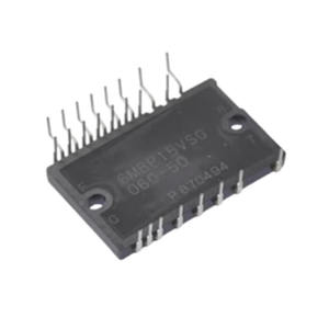
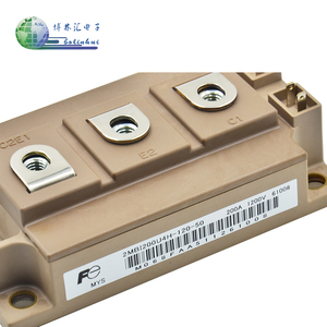
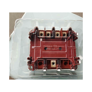
As global microelectronics fabrication transitions toward sub-3nm nodes, power delivery networks (PDN) within semiconductor manufacturing tools require unprecedented levels of electrical stability, thermal efficiency, and harmonic mitigation. Operating at the intersection of material science and applied power electronics, our manufacturing facilities stand as China’s leading authority in advanced power semiconductor packaging, wafer synthesis, and modular power conversion.
Building upon over 60 years of combined power engineering expertise—and rigorously operated under certified ISO 9001:2015 and ISO 13485 quality management systems—our production architecture enforces zero-defect manufacturing standards. From high-purity single-crystal silicon ingot growth (Czochralski and Magnetic Czochralski methods) to high-voltage Direct Copper Bonding (DBC) ceramics, every step in our process chain is monitored via real-time statistical process control (SPC).
Unlike secondary assembly vendors, our manufacturing campus maintains complete internal control over silicon substrate sizing, epitaxy layer growth, wire bonding, transfer molding, and automated high-voltage isolation testing. Every individual power module undergoes 100% full-load functional burn-in and dynamic switching isolation verification before international dispatch.
Our R&D divisions independently design custom gate driver ICs, magnetic transformers, and specialized topologies (including soft-switching Zero Voltage Switching phase-shifted full-bridge converters). We eliminate reliance on external third-party intellectual property, enabling rapid customization for custom mechanical form factors and bespoke electrical specifications.
Semiconductor fab uptime depends on rigorous adherence to international standards. Our capital equipment power supply platforms are pre-tested for complete compliance with SEMI F47 (voltage sag immunity), IEC 60601-1 3rd Edition (2xMOPP) for medical-grade isolation, and CISPR 11 / FCC Class A conducted noise standards.
Comparative technical benchmarks across our core power semiconductor packaging series engineered for semiconductor fabrication equipment, high-voltage inverters, and heavy-duty industrial automation.
| Module Topology | Voltage Rating ($V_{CES}$) | Current Rating ($I_C$) | Thermal Resistance ($R_{th(j-c)}$) | Cooling Paradigm | Primary Fab Application |
|---|---|---|---|---|---|
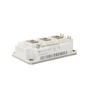
| FF200R12KE3 Dual IGBT | 1200 V | 200 A | 0.12 K/W | Forced Air / Conduction | High-Power Inverters & DC Drives |
| 6MBP15VSG060-50 6-in-1 IPM | 600 V | 15 A | 0.85 K/W | Convection / Heatsink | Precision Wafer Handling Robotics |
| SKIM455GD12T4DM1 Half-Bridge | 1200 V | 450 A | 0.045 K/W | Direct Liquid Cold Plate | Substation & MW Fab Power Systems |
| XNG50PI24TC3S3 Inverter | 2400 V | 50 A | 0.18 K/W | Closed-Loop Liquid Cooled | RF Generators & Plasma Etch Systems |
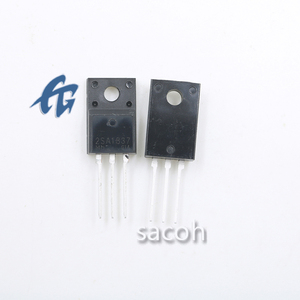
| SACOH A1837 / C4793 MOSFET Pair | 230 V | 1.5 A | 1.25 K/W | PCB Copper Plane / Air | Electrostatic Chuck Gate Drivers |
The global power semiconductor procurement landscape is undergoing a structural paradigm shift driven by the rapid commercialization of Wide-Bandgap (WBG) materials, the demand for unprecedented power density inside cleanroom footprints, and supply chain diversification imperatives. Global procurement officers and engineering leads must align their sourcing strategies with four critical technological trends:
While standard Silicon (Si) IGBTs remain workhorses for high-current low-frequency applications, procurement volumes for 1200V SiC MOSFETs and 650V GaN HEMTs are escalating rapidly. SiC’s 10x higher breakdown electric field strength allows for significantly thinner drift layers, cutting conduction losses ($R_{DS(on)}$) by up to 70% at elevated junction temperatures ($T_j > 175^\circ\text{C}$). Fabs specifying SiC power modules achieve dramatic footprint reductions in plasma generator racks.
Traditional forced-air cooling introduces turbulent air patterns and potential dust contamination inside ISO Class 1 semiconductor cleanrooms. Modern procurement specifications prioritize direct liquid-cooled (DLC) power supplies. Liquid cooling removes thermal energy up to 4x more efficiently than air, enabling 16.5 kW power delivery in compact 1U rack dimensions while entirely eliminating noisy, failure-prone cooling fans.
A single voltage sag lasting just 100 milliseconds can cause a tool abort in lithography or chemical vapor deposition (CVD) equipment, resulting in hundreds of thousands of dollars in ruined wafer inventory. Purchasing teams now mandate verified SEMI F47 compliance, requiring power conditioning units to hold regulated DC output voltage through single-phase voltage sags down to 50% of nominal input for up to 200 ms.
Analog-only power converters are being phased out in favor of digital power platforms integrated with PMBus, CANopen, or EtherCAT communications. Intelligent gate drivers stream microsecond-level telemetry—monitoring collector-emitter saturation voltage ($V_{CE(sat)}$), real-time die junction temperature ($T_j$), and leakage currents—enabling predictive maintenance before cataclysmic semiconductor breakdown occurs.
Designing high-reliability power electronics for semiconductor tool capital equipment demands continuous innovation across material chemistry, thermal management, and parasitic inductance mitigation. The following technological breakthroughs represent the core of our manufacturing capabilities:
In high-power IGBT and SiC modules, high rate of current change ($di/dt$) during turn-off creates severe inductive voltage spikes ($V_{spike} = L_{stray} \times di/dt$). By utilizing laminated copper busbar internal structures and symmetrical die positioning on Direct Copper Bonding (DBC) ceramic substrates, our package engineers have reduced internal stray inductance ($L_{stray}$) to under 15 nH. This allows engineers to push switching frequencies higher without risking reverse-bias safe operating area (RBSOA) breakdown.
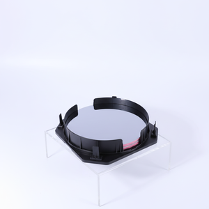
The performance of high-power discrete devices begins at the wafer substrate level. Traditional Czochralski (CZ) pulling often introduces micro-defects and oxygen precipitates that degrade breakdown voltage uniformity. Our Magnetic Czochralski (MCZ) growth process applies a strong magnetic field to the molten silicon crucible, suppressing thermal convection currents. This yields 6-inch silicon wafers with exceptionally uniform radial resistivity, low oxygen content ($< 1 \times 10^{17}\text{ atoms/cm}^3$), and near-zero crystal-originated pits (COPs).
Conventional lead-tin or lead-free soldering between the semiconductor die and baseplate exhibits solder-fatigue voids after thermal cycling. Our high-power module packaging utilizes solid-state silver sintering under high pressure. Silver sintering provides a melting point of $961^\circ\text{C}$ (far above operating limits) and a thermal conductivity of $> 200\text{ W/m}\cdot\text{K}$ (compared to $\approx 50\text{ W/m}\cdot\text{K}$ for standard solder), increasing module thermal cycling lifespan by more than 5x.
Technical and commercial guidance provided directly by our senior applications engineering team.
SEMI F47 is an industry standard specifying the minimum voltage sag ride-through capability for equipment used in semiconductor microchip fabrication. A compliant power supply must continue to deliver fully regulated DC voltage during utility voltage sags—such as a drop to 50% line voltage for 200 milliseconds, or 70% line voltage for 500 milliseconds. Compliant supplies incorporate enhanced bulk energy storage capacitance and adaptive PWM control loops, preventing costly fab tool shutdowns and wafer scrapping during transient utility grid disruptions.
While standard Czochralski (CZ) thermal pulling is cost-effective for general microelectronics, natural thermal convection within the silicon melt introduces variations in oxygen concentration and dopant distribution. Magnetic Czochralski (MCZ) applies a strong horizontal or vertical magnetic field during crystal pulling, damping fluid motion in the melt. This results in significantly lower interstitial oxygen content, superior micro-defect control, and tight radial resistivity distribution—making MCZ wafers essential for high-voltage IGBTs, high-current MOSFETs, and power thyristors.
Selecting between Delta and WYE EMI filter topologies depends entirely on the electrical line distribution. A 3-Phase Delta filter is designed for 3-wire systems without a neutral conductor, filtering line-to-line differential-mode noise. A 3-Phase WYE filter is engineered for 4-wire systems containing a neutral conductor. WYE filters provide filtering across line-to-neutral paths as well as common-mode noise to earth ground. Installing a Delta filter on a 4-wire network leaves line-to-neutral noise unattenuated, risking CISPR 11 conducted emissions compliance failures.
Liquid cooling offers a volumetric heat transfer coefficient up to 1,000 times greater than air convection. This allows power supplies to operate at dramatically higher power densities (e.g., 16.5 kW in a 1U chassis) while keeping semiconductor junction temperatures ($T_j$) low. Furthermore, liquid cooling eliminates cooling fans, removing the primary electro-mechanical point of failure, eliminating fan noise, and preventing dust or particulate dispersion inside ISO Class 1 cleanroom environments.
Standard industrial IGBT modules typically feature basic isolation ($1.5\text{kV AC}$ to $2.5\text{kV AC}$). Medical equipment requires 2xMOPP (Means of Patient Protection) safety isolation with $4.0\text{kV AC}$ dielectric withstand and ultra-low earth leakage currents ($< 300\,\mu\text{A}$). Adapting an industrial module requires adding secondary isolation transformers, optocoupled gate drivers certified to UL 1577, and potted high-dielectric DBC ceramics. Our custom engineering team provides turnkey modifications to elevate industrial power platforms to IEC 60601-1 or MIL-STD-461 standards.
For modified standard modules (e.g., custom pinout lengths, specialized thermistors, or custom baseplates), typical engineering prototyping requires 4 to 6 weeks. Ground-up custom power module packaging (involving custom DBC layout and transfer mold tooling) ranges from 10 to 14 weeks. Every custom program follows a structured APQP gate process: design review, thermal simulation, pre-compliance testing, sample delivery, customer qualification, and automated mass-production ramp-up.
Whether you require high-purity single-crystal silicon wafers, standard IGBT inverter modules, or fully custom SEMI F47 compliant liquid-cooled power supplies, our senior application engineering team is ready to review your schematics, thermal budgets, and compliance specs.
