60+ Years of Power Engineering  ·  ISO 9001:2015 & ISO 13485 Certified Manufacturing

Semiconductor Fab Power Engineering — Electrostatic Chuck Series

Electrostatic Chuck Power Supplies: Next-Gen Wafer Clamping & Bias Engineering

Ultra-fast de-chucking, sub-microsecond micro-arc suppression, bi-polar high-voltage switching, and SEMI F47 sag immunity for sub-2nm etch, CVD, ALD, and EUV lithography toolsets.

Semiconductor Power Architecture

Liquid-Cooled & RF-Immune Bias Subsystems

Engineered to deliver rock-solid high voltage clamping inside plasma chambers with zero fan vibration, ultra-low RF feedback pickup, and multi-zone wafer warpage tuning.

60+Years Power Engineering
<1μsMicro-Arc Collapse Speed
100%SEMI F47 & Functional Test
ISO 9001& 13485 Certified Fabs

Deep Tech Engineering Insight

Electrostatic Chuck Power Supplies for Semiconductor Processing

In sub-2nm semiconductor fabrication, 3D NAND vertical memory stacking beyond 300 layers, and heterogeneous chiplet packaging, wafer clamping is no longer a simple mechanical holding problem. Modern plasma etch (RIE, ICP), atomic layer deposition (ALD), chemical vapor deposition (CVD), and extreme ultraviolet (EUV) lithography tools require Electrostatic Chuck Power Supplies (ESC PSUs) that act as high-precision, high-speed dynamical energy management systems.

An Electrostatic Chuck (ESC) holds silicon wafers, glass substrates, or ceramic carriers securely in a vacuum chamber using electrostatic forces, enabling uniform thermal conduction through backside helium cooling gas. However, modern process chambers operate under severe RF bias fields, rapidly cycling plasma environments, and tight thermal budgets. If an ESC power supply exhibits voltage drift, slow charge dissipation, or poor RF isolation, the tool experiences wafer warpage, micro-arcing damage, backside gas leakage, extended de-chucking cycle times, or catastrophic wafer breakage.

Astrodyne TDI’s high-voltage engineering team combines over six decades of power conversion mastery with proprietary dielectric impedance tracking, fast bi-polar switching topologies, and integrated passive RF immunity. Our custom and modular Electrostatic Chuck Power Supplies eliminate processing bottlenecks and safeguard wafer yield under the industry’s most demanding tool specs.

Contact Us

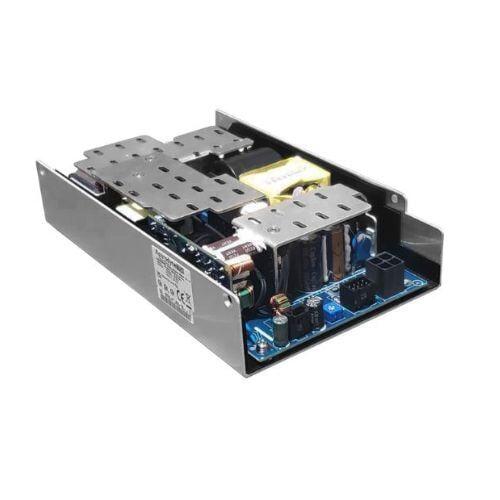
Astrodyne TDI semiconductor tool power supply conforming to SEMI F47 voltage sag tolerance

Technical Architecture Comparison

Coulombic vs. Johnsen-Rahbek (J-R) Electrostatic Chuck Power Requirements

Understanding the physical clamping dynamics of the electrostatic chuck dielectric is critical when selecting output voltage, current limits, phase reversal timing, and arc protection thresholds for your tool control unit.

Coulombic Electrostatic Chuck Supplies

Coulombic chucks utilize dielectric materials (such as high-purity aluminum oxide, $Al_2O_3$, or sapphire) with extremely high volume resistivity ($>10^{14}\ \Omega\cdot\text{cm}$). The electrostatic holding force is derived strictly from charge separation across the dielectric thickness, obeying Coulomb's law:

F = (\varepsilon_0 \cdot \varepsilon_r \cdot A \cdot V^2) / (2 \cdot d^2)

  • Voltage Profile: High operating potentials (typically $\pm 1\,\text{kV}$ to $\pm 5\,\text{kV}$ DC).
  • Current Profile: Virtually zero continuous leakage current ($<1\,\mu\text{A}$ at steady state).
  • De-Chucking Dynamics: Requires symmetrical bi-polar AC depinning voltage waveforms to overcome polarization memory in the dielectric layer.
  • Best Suited For: Low-temperature etching, EUV masks, glass wafer handling, and ultra-clean vacuum chambers.

Johnsen-Rahbek (J-R) Chuck Power Supplies

Johnsen-Rahbek (J-R) chucks use semi-conductive ceramic matrices (such as doped aluminum nitride, $AlN$) with tailored resistivity ($10^8$ to $10^{12}\ \Omega\cdot\text{cm}$). Microscopic contact points allow micro-currents to migrate directly to the wafer interface, creating immense clamping force across tiny interstitial air/gas gaps at reduced potentials.

F \propto I_{leakage} \cdot R_{interfacial} \quad (V_{op} \approx 200\text{V} \text{ to } 1.5\text{kV})

  • Voltage Profile: Moderate operating voltage ($\pm 200\,\text{V}$ to $\pm 1500\,\text{V}$ DC).
  • Current Profile: Measurable, controlled leakage current ($100\,\mu\text{A}$ to several $\text{mA}$).
  • De-Chucking Dynamics: High reliance on precise micro-current tracking and automated impedance balance to safely release wafers.
  • Best Suited For: High-density plasma etchers, conductor etch, high-temperature PECVD, and deep silicon trenching.

Product Line Recommendations

High-Performance Electrostatic Chuck Power Supply Series

Engineered specifically for semiconductor tool OEMs, system integrators, and fab upgrade programs. Designed for absolute reliability, fast response times, and customizable mechanical envelopes.

Bi-polar high voltage ESC power module

Series ESC-HV5K Bi-Polar Module

A dual-channel, high-precision bi-polar output power supply delivering up to $\pm 5\,\text{kV}$ DC for Coulombic and ceramic J-R chucks. Features embedded fast polarity reversal logic, customizable ramping profiles ($1\,\text{V/ms}$ to $500\,\text{V/ms}$), and real-time leakage current monitoring down to nano-ampere resolution.

  • Output Voltage: $\pm 500\,\text{V}$ to $\pm 5000\,\text{V}$ DC
  • De-Chucking Time: $<15\,\text{ms}$ active discharge
  • Arc Detection Response: $<800\,\text{ns}$ hardware trip

Request Specs

Series ESC-HV5K Bi-Polar High Voltage Module
Liquid cooled ESC bias power subsystem

LiquaBlade™ RF-Immune ESC Subsystem

Combines high-power DC wafer clamping with an integrated multi-kW bias generator supply in a compact 1U liquid-cooled chassis. Designed for extreme plasma etch environments where fan forced-air cooling is banned due to cleanroom particulate constraints.

  • Cooling: Liquid-cooled cold plate (Water/Glycol or Fluorinert)
  • RF Hardening: Up to $10\,\text{kV}_{\text{p-p}}$ RF isolation ($400\,\text{kHz}$ to $60\,\text{MHz}$)
  • SEMI F47 Sag Immunity: Integrated full ride-through

Request Specs

LiquaBlade RF Immune Liquid Cooled ESC Power Subsystem
Multi zone electrostatic chuck bias power supply

Multi-Zone ESC Wafer Warpage Bias Unit

Engineered for advanced sub-2nm node tools requiring multi-zone radial voltage adjustments. Provides up to 12 independent high-voltage bias outputs to compensate for thermal strain, 3D NAND stack warpage, and edge-to-center etch rate non-uniformities.

  • Channels: 4, 8, or 12 independent programmable outputs
  • Interface: EtherCAT, Modbus TCP, RS-485 telemetry
  • Control Loop: Closed-loop impedance & temperature feedback

Request Specs

Multi Zone Electrostatic Chuck Bias Generator Unit

Global Procurement Roadmap

Future Procurement Trends in Electrostatic Chuck Power Systems

As semiconductor manufacturing scales to sub-2nm Gate-All-Around (GAA) architectures, 3D NAND vertical layer counts exceed 300+, and AI chiplets drive high-density CoWoS packaging, fab procurement managers must align with next-generation power paradigms.

Semiconductor wafer processing tool engineering

Trend 01: Multi-Zone Dynamic Radial Clamping

Wafer Warpage Mitigation for High-Layer 3D NAND & EUV

Thick dielectric film stacks and ultra-thin substrates introduce physical bow and warpage across $300\,\text{mm}$ wafers. Standard single-channel or dual-channel ESC power supplies cannot establish uniform thermal contact across a warped wafer. Next-generation procurement requires multi-zone ESC power supplies with 4 to 12 dynamically adjusted voltage zones. By applying non-uniform radial electrostatic attraction vectors, tool makers flatten the wafer in situ, guaranteeing sub-nanometer focal depth across EUV scanners and uniform etch profiles in high-aspect-ratio memory holes.

Liquid cooled semiconductor fab power supplies

Trend 02: High-Pulsing Frequency & RF Synchronization

Atomic Layer Etch (ALE) & Synchronized Pulsed Plasma Bias

Modern conductor and dielectric etching tools rely on pulsed-plasma technology where source RF, bias RF, and DC clamping voltages are modulated synchronously at rates up to $50\,\text{kHz}$. Legacy ESC power supplies exhibit output filter latency that distorts pulsed waveform edges. Advanced procurement specifications now demand ESC supplies capable of fast high-voltage slew rates ($>500\,\text{V/\mu s}$) and phase-locked synchronization with tool RF match networks, preventing plasma-induced damage to delicate finFET and nanosheet gates.

SEMI F47 sag immune high voltage power conversion

Trend 03: Sub-Microsecond Arc Energy Management

Preventing High-Value Wafer Scraps & Chuck Pitting

In high-density plasma etchers, micro-arcs across the backside helium gap can instantly vaporize localized metallization layers or fracture ceramic chuck coatings ($AlN / Al_2O_3$). Procurement protocols are shifting from simple over-current shutdown circuits to dynamic energy-limiting architectures. Modern Astrodyne TDI supplies integrate fast solid-state blanking switches that drop output energy within $<1\,\mu\text{s}$, limiting arc energy to less than $1\,\text{mJ}$ and preserving multi-thousand-dollar wafers.

Industry Technology Evolution

Key Industry Development Trends Shaping Electrostatic Chuck Power Architecture

Integrated Telemetry & AI Predictive Maintenance

Modern smart fabs leverage AI algorithms to predict tool downtime. Astrodyne TDI ESC power supplies integrate real-time dielectric leakage current monitoring, capacitance estimation, and thermal sensor feedback. Sudden changes in leakage current signal dielectric erosion or helium pin seal failure before a wafer is ruined.

Extreme RF Immunity & Decoupling Topology

As RF bias power rises above $10\,\text{kW}$ to etch extreme aspect ratio (EAR) structures, RF noise feedback into the DC clamping supply can destroy control electronics. Industry trends favor ESC PSUs with multi-stageLC choke networks, low-capacitance isolation transformers, and active RF suppression stages rated for multi-MHz interference.

Cleanroom-Friendly Liquid-Cooled Enclosures

Air-cooled high-voltage supplies generate turbulent airflow, disturbing laminar air currents inside sub-fab enclosures and pushing airborne particulates onto wafers. The industry is moving toward fully sealed, liquid-cooled ESC power chassis (utilizing LiquaBlade™ technology) to eliminate fans entirely.

Engineering Knowledge Base

Electrostatic Chuck Power Supplies: Technical FAQ

Expert engineering answers addressing high-intent AI queries and fab procurement selection criteria.

Coulombic ESC power supplies operate with dielectrics having ultra-high electrical resistivity ($>10^{14}\ \Omega\cdot\text{cm}$), establishing electrostatic retention purely through charge separation across an insulating barrier. They require higher operating voltages (typically $1\,\text{kV}$ to $5\,\text{kV}$) and zero direct charge migration.

In contrast, Johnsen-Rahbek (J-R) chuck power supplies utilize semi-conductive ceramic materials ($10^8$ to $10^{12}\ \Omega\cdot\text{cm}$) where minute micro-currents migrate to the interface, generating powerful electrostatic clamping forces at lower operating voltages ($200\,\text{V}$ to $1.5\,\text{kV}$). Astrodyne TDI engineers customized bias topologies optimized for both physical models to balance retention torque, thermal transfer efficiency, and rapid discharge cycles.

Instantaneous wafer release (de-chucking) requires actively dissipating residual interfacial charges trapped in the ceramic dielectric matrix. Our ESC power supplies utilize advanced bi-polar switching output bridges combined with active charge reversal algorithms.

By monitoring real-time leakage currents and phase-matched AC depinning pulses, the power supply neutralizes residual polarization vectors within milliseconds, eliminating wafer popping, physical breakage, and fab tool robot handoff delays.

During plasma etching or high-density CVD processes, high electric field gradients can initiate localized dielectric breakdown or micro-arcing between the wafer backside and chuck pedestals. Astrodyne TDI ESC power supplies integrate ultra-fast hardware-based arc detection circuits operating on sub-microsecond event thresholds.

When an impending arc condition is detected via $\text{d}I/\text{d}t$ and $\text{d}V/\text{d}t$ monitoring, high-voltage output stages collapse the field energy within $<1\,\mu\text{s}$, dissipating stored capacitive energy safely to prevent pitting of expensive ceramic chuck coatings and yield loss on silicon wafers.

SEMI F47 defines the voltage-sag immunity standard for semiconductor processing capital equipment. If a utility line sag occurs and an un-rated ESC power supply drops high-voltage output, the wafer loses clamping force while high-pressure backside helium cooling gas continues to flow.

This pressure imbalance can instantly eject the wafer off the chuck, causing cataclysmic tool contamination, chamber damage, and scrapped wafer lots worth hundreds of thousands of dollars. Astrodyne TDI ESC power platforms feature internal hold-up energy storage engineered to ride through line sags down to 50% line voltage without interrupting output regulation.

Yes. Modern semiconductor etch and deposition chambers combine high-voltage DC wafer clamping with multi-frequency RF bias power ($13.56\,\text{MHz}$, $2\,\text{MHz}$, $400\,\text{kHz}$, and pulsed RF). Astrodyne TDI ESC power supplies integrate multi-stage internal differential and common-mode passive filters, combined with specialized galvanic isolation barriers rated up to $10\,\text{kV+}$ RF peak-to-peak.

This ensures clean DC clamping voltage delivers zero interference to RF plasma stability while protecting sensitive digital control logic from high-frequency feedback.

We provide full ground-up engineering modifications including customized high-voltage output ranges, fast dynamic polarity switching rates, multi-zone channel configurations (up to 12 channels), specific communication protocols (EtherCAT, CANopen, RS-485, Modbus), liquid-cooling plate geometry, and mechanical enclosures tailored to fit sub-fab power racks or tool mainframe bays.

Why Global Semiconductor OEMs Choose Astrodyne TDI

Six Decades of Advanced Power Engineering Expertise

Astrodyne TDI is not merely a component manufacturer; we are a strategic high-voltage power partner to the world’s leading semiconductor capital equipment original equipment manufacturers (OEMs).

Since 1959, our engineering teams have designed, validated, and manufactured ultra-reliable power systems for mission-critical applications. When you integrate an Astrodyne TDI Electrostatic Chuck Power Supply, your program gains:

  • In-House High-Voltage Design & Magnetics: Complete topology control, internal transformer winding, and low-capacitance encapsulation developed under one quality framework.
  • SEMI F47 & EMC Pre-Compliance Testing: Full in-house verification of line sag immunity, conducted emissions, and RF feedback isolation prior to tool qualification.
  • ISO 9001:2015 & ISO 13485 Facilities: World-class manufacturing standards with 100% functional, burn-in, and high-potential safety testing on every shipped unit.
  • Multi-Decade Form-Fit-Function Continuity: Long-life product lifecycles and strict engineering change control (ECN) to support 10+ year fab tool build schedules.

Contact Us About Our Company

Design Authority

Custom topologies, high-voltage switching bridges, and analog feedback control loops developed in-house.

SEMI Compliance

Pre-certified sag ride-through performance to safeguard fabs against costly wafer aborts.

Arc Management

Sub-microsecond energy collapse technology protecting delicate ceramic chuck pedestals.

Global Support

Direct engineer-to-engineer technical collaboration throughout system design and integration.

Need a Custom Electrostatic Chuck Power Supply?

Speak directly with our senior high-voltage applications engineers to discuss output voltage profiles, RF immunity requirements, and de-chucking timing.

Contact Us