Discover our industry-standard power conversion modules, high-voltage switching supplies, and custom bias platforms engineered specifically for semiconductor fab tools and electrostatic clamping assemblies.
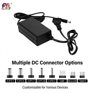
Regulated auxiliary power adapter with multi-region AC plugs (US/EU/UK/AR). Engineered for stable low-noise powering of ESC digital logic controllers, sensor diagnostic arrays, and vacuum chamber monitoring units.
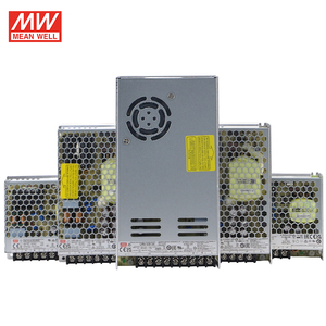
Industrial-grade switching power supplies ranging from 5A to 60A output. Highly reliable DC supply designed to handle intense electromagnetic interference inside plasma etching and deposition chambers.
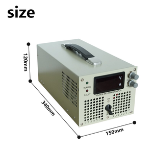
High-efficiency (88-89%) adjustable DC source from 12V up to 600V with integrated overcurrent protection. Perfect for dynamic electrostatic electrode polarization and laboratory wafer clamping R&D setups.
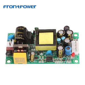
Customizable open-frame PCB power supply boards supporting multi-rail voltage output (12V, 15V, 24V, 48V). Tailored for embedded incorporation into compact ESC dynamic temperature-control sub-racks.

Digital benchtop regulated DC switching power source featuring low ripple, ultra-fine resolution adjustment, and fast transient response for wafer chuck voltage breakdown calibration tests.
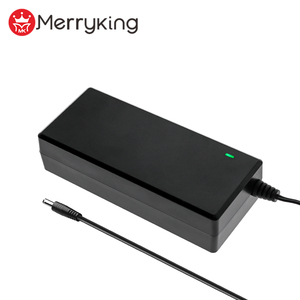
Compact high-wattage desktop adapters with multi-current options (up to 15A output). Ideal for powering external helium backside leak detectors and motorized chuck lift-pin assemblies.
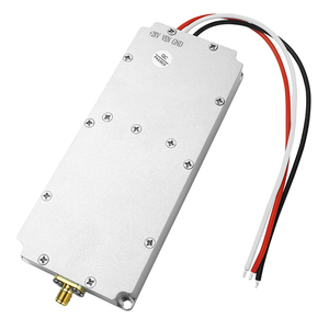
Heavy-duty industrial power converter built with premium EMI suppression stages. Ensures zero line disruption and strict compliance with SEMI F47 voltage sag immunity standards.
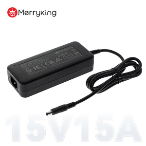
Flexible output (12V to 48V) industrial desktop power supply designed for high thermal stability, long service life, and 24/7 uninterrupted fab tool operational demands.
In sub-2nm semiconductor manufacturing, the Electrostatic Chuck (ESC) is far more than a simple mechanical fixture—it is an intricate, multi-physics thermal and electrical interface critical to plasma etch, physical vapor deposition (PVD), chemical vapor deposition (CVD), and EUV lithography systems.
An Electrostatic Chuck holds semiconductor wafers in place using electrostatic force generated by high-voltage DC bias applied across a dielectric layer (typically High-Purity Aluminum Nitride, AlN, or Aluminum Oxide, Al2O3). This non-mechanical clamping technique prevents edge deformation, eliminates particle generation associated with mechanical clamps, and allows uniform helium backside gas distribution for micro-degree temperature control across 300mm silicon wafers.
To meet aggressive yield targets, leading semiconductor OEMs require complete integration between the ceramic chuck substrate, embedded heating zones, and high-frequency pulsed DC power supplies equipped with ultra-fast micro-arc detection routines.
Choosing the right electrostatic attraction mechanism depends directly on chamber operating temperature, plasma chemistry, and target wafer resistivity.
| Technical Parameter | Coulombic Electrostatic Chuck | Johnsen-Rahbek (J-R) Electrostatic Chuck |
|---|---|---|
| Primary Mechanism | True electrostatic capacitor separation; dielectric acts as pure insulator ($\rho > 10^{14} \ \Omega\cdot\text{cm}$). | Controlled charge transport through semi-conductive dielectric ($\rho \approx 10^{9} - 10^{11} \ \Omega\cdot\text{cm}$). |
| Clamping Force Density | Moderate force ($10 - 40 \ \text{kPa}$). Highly stable across temperature ranges. | Ultra-high force ($50 - 150+ \ \text{kPa}$) at small micro-gap distances. |
| Dielectric Material | High-Purity Sapphire, Al2O3, or high-resistivity AlN. | Doped Aluminum Nitride (AlN with Titanium/Iron dopants). |
| Residual Charge Residuals | Extremely low residual charge; immediate mechanical de-clamping. | Requires reverse-polarity pulsing voltage to quickly discharge accumulated J-R interface ions. |
| Best Application Suitability | EUV Lithography, Low-temperature Etch, PVD, Metrology inspection tools. | High-temperature PECVD, High-Density Plasma (HDP-CVD), Advanced HAR Etch. |
As semiconductor node scaling advances toward 1nm and gate-all-around (GAA) 3D transistor architectures become ubiquitous, electrostatic chuck procurement is undergoing major technological shifts.
Traditional dual-zone (inner/outer) chucks can no longer meet the strict critical dimension (CD) uniformity required for EUV double-patterning. Procurement is pivoting toward multi-zone ceramic ESCs featuring 32 to 64+ embedded micro-heaters driven by fast-switching, high-density modular DC power supplies. This allows real-time local thermal profiling to offset plasma non-uniformity.
Atomic Layer Etching (ALE) and High Aspect Ratio (HAR) memory hole etching require rapid modulation of wafer bias. Procurement officers are specifying power systems capable of sub-millisecond reverse-polarity voltage ramping, micro-second arc suppression, and active capacitive discharge algorithms to protect expensive wafers from micro-arc cratering.
Fab cleanroom space commands a premium price per square meter. The semiconductor industry is aggressively moving away from air-cooled power racks in favor of high-density liquid-cooled power platforms (such as LiquaBlade™ architectures). Removing internal cooling fans prevents air turbulence, eliminates particle contamination, and shrinks 16.5kW power blocks into standard 1U sub-racks.
With over 60 years of engineering innovation, Astrodyne TDI stands as a premier design authority and manufacturer of custom AC/DC power supplies, high-voltage switching modules, and EMI/EMC line filters for mission-critical semiconductor capital equipment.
Our engineering team bridges the gap between complex plasma chamber physics and reliable electrical conversion. From modified standard power supplies to fully customized ground-up power subsystems, we ensure full compliance with rigorous sector requirements including SEMI F47 line sag immunity, ISO 9001:2015, and ISO 13485 quality standards.
Custom high-voltage transformers and RF isolation chokes optimized specifically for electrostatic bias applications.
Guaranteed ride-through performance during utility line voltage sags, preventing tool aborts and protecting wafer yields.
Every power unit undergoes rigorous thermal cycling, high-pot isolation tests, and dynamic load testing prior to shipment.
Direct engineer-to-engineer collaboration from initial concept specification through qualification and long-life manufacturing.
Essential guidance on selecting electrostatic chuck suppliers, matching power supply topologies, and ensuring process tool reliability.
Key selection criteria include: (1) Dielectric Material Quality: Purity and density of Aluminum Nitride (AlN) or Al2O3 to guarantee consistent dielectric constant ($\epsilon_r$) and breakdown strength over millions of process cycles; (2) Thermal Management Expertise: Ability to integrate multi-zone resistive heaters and helium backside cooling channels with sub-degree temperature gradient precision; (3) RF & DC Power Compatibility: Co-engineering capability ensuring the chuck assembly works seamlessly with high-voltage DC bias supplies and high-frequency RF matching networks without electrical breakdown; and (4) Manufacturing Cleanliness: ISO Class 5 cleanroom assembly and 100% helium leak testing capability.
SEMI F47 defines the voltage sag immunity requirement for semiconductor processing tools. If an incoming AC utility line suffers a short-duration voltage drop, a non-compliant power supply driving the ESC may trip or lose clamping bias. This loss of electrostatic attraction causes instant loss of backside helium pressure, leading to wafer overheating, severe thermal stress, wafer scrapping, and emergency process tool aborts. Our custom power solutions incorporate robust hold-up energy storage and optimized power factor correction (PFC) stages to guarantee zero interruption during SEMI F47 line sag events.
During plasma etching or deposition, localized gas breakdown or dielectric defects can ignite severe electrical micro-arcs between the wafer and the chuck electrodes. If unmitigated, these arcs permanently pit the expensive ceramic chuck surface and destroy micro-circuitry on the active silicon wafer. Modern ESC power supplies must feature high-speed solid-state switching circuits that detect sudden current spikes ($\frac{di}{dt}$) and shut down or quench the high voltage in less than 1 millisecond, safely dissipating residual energy before catastrophic damage occurs.
Liquid cooling eliminates internal fans, which are a primary source of mechanical vibration, acoustic noise, and particulate circulation inside cleanroom environments. Liquid cooling also provides vastly superior thermal transfer, allowing kilowatt-class power conversion modules (such as LiquaBlade™ platforms) to achieve extreme power density in compact 1U sub-racks. This frees up critical cabinet volume inside plasma tool bays while maintaining lower junction temperatures for power semiconductors, dramatically extending equipment MTBF (Mean Time Between Failures).
Yes. While off-the-shelf power supplies provide standard DC outputs, electrostatic chuck applications often require custom high-voltage ramping profiles, dual bipolar outputs ($\pm 1500\text{V}$ to $\pm 5000\text{V}$), fast polarity reversing, and integrated high-frequency RF filter networks. Astrodyne TDI specializes in modifying proven power platforms or building custom-engineered power subsystems tailored to your specific mechanical envelope, digital communications protocol (EtherCAT, Modbus, RS-485), and safety interlock requirements.
Whether you require standard auxiliary power adapters, SEMI F47 compliant switching supplies, or custom high-voltage electrostatic chuck bias platforms, our senior applications engineering team is ready to assist.
